Today I was able to reach wch-ic.com. wch.cn and mounriver.com. No telling if it had anything to do with the approaching Lunar New Year as celebrated in China and many other parts of the world or not.
I have taken the opportunity to upgrade to the latest CH32V003 RM V1.7, dated 2024-03-11.
So now I’m back to wondering why the GNU RISC-V assembler treats pseudo-instructions differently based on the destination register involved. Specifically, why does it it produce this:
la sp, _eusrstack # initialize the stack pointer
0: 20005117 auipc sp,0x20005
4: 00010113 mv sp,sp
la sp, 0x20005000 # *** debug *** for comparison
8: 20005137 lui sp,0x20005
lui sp, %hi(_eusrstack) # initialize the stack pointer
c: 20005137 lui sp,0x20005
la t0, _eusrstack # *** debug *** for comparison
10: 20005297 auipc t0,0x20005
14: ff028293 addi t0,t0,-16 # 20005000 <_eusrstack>
la t0, 0x20005000 # *** debug *** for comparison
18: 200052b7 lui t0,0x20005
So one thing I see is that when I reference the linker variable _eusrstack, it always uses the auipc+mv combination, whereas when I use the immediate value 0x20005000, it uses the single instruction lui (load upper [20 bits] immediate).
I don’t know if it has anything to do with anything, but it now feels like the time has come to deploy my own linker script. Not to worry, it’s already written and around here… somewhere.
I found four of them, for the 003, 203, 208 (just a copy of the 003) and 307. I’ll use the 307 as a basis and make a few changes, as appropriate.
Now here’s an issue I had not previously considered. The 003 only offers one memory configuration: 16KB flash ‘rom’ and 2KB SRAM. So a single linker script applies to the entire family.
It turns out that this is also the case for the CH32X035 line, all the way from the smallest (F) to the largest (R) packages offered: 62KB flash ‘rom’ and 20KB SRAM. So for today I don’t need to figure out how to accurately specify memory capacities in linker scripts for the larger parts, such as the 203, 208 and 307. [TODO]
OK, today’s tangent is to find out why or how the CH32X035F8U6 device in QFN20 package offers 19 GPIO. I have a stack of these as realized as the WeAct core boards.
Well, it’s true! They are using the bottom pad as the single, only solitary ground reference connection. This is also the case for the CH32X035G8U6 device that I am currently examining.
I’m not sure how I feel about this. Mostly, I’m glad this tangent was so quickly ended.
Note: Just make really sure to properly ground these parts when laying out a PCB. This effectively rules out their use on single-sided PCBs.
Small changes to the linker script:
Update header and footer with current date and new filename
Change ENTRY(start) to ENTRY(_start)
Adjust flash and RAM sizes as needed
Now it’s time to change the project settings to use the newly-available linker file, which I have added to the CH32X035/lib folder.
The MRS2 build options seem to expect the linker script to reside within the project folder, which is how it was and was working just fine. The two options for the linker script in the ‘Open the file from:’ option were Project or Local Folder. I’ll try a relative reference in the Project option first: ../inc/CH32X035.ld
Well, it didn’t like it: “ld: read in flex scanner failed”
But nowhere do I see a reference to the linker script in the command line invocation. Now the sharp-eyed amongst you will have seen my (now) obvious error: I referenced the ‘inc’ folder, not the ‘lib’ folder.
Once again, it needed an addition level of redirection, because the source code is within a project sub folder, so the proper entry is “../../lib/CH32X035.ld” in the linker settings.
Now it is rightfully complaining about an “undefined reference to `_eusrstack'”. So I will make the proper adjustment, substituting ‘end_of_RAM’ for ‘_eusrstack’ and see what happens.
Hey, it works. Waddaya know? Also, the mysterious ‘2048’ bytes of BSS are gone from the size totals summary, as they were a nod to the 2K allocated to the stack in the original linker script.
To get an assembler listing that includes the source code but does not include a lengthy list of all the defined symbols (there are a LOT of them from the include file), use these options:
NOT the 'Generate assembler listing..." from Assembler/Misc
NOT the 'Generate assembler listing..." from Compiler/Misc
Only these three (3) from  GNU RISC-V Cross Create Flash Listing/General
    Create extended listing
    Display source
    Disassemble
A very tidy listing, indeed.
Note: Leave some sort of debugging information available, i.e., don’t use Debugging: None option, or guess what? It won’t let you debug! I mean, it does, but doesn’t show you where you are at the moment as you step through the code.
So that was a nice step in the right direction. I can now delete the ‘Ld/‘ project sub-folder and the provided linker script, and the project still builds, flashes, runs and debugs as expected.
So the behavior of the assembler remains the same: the references to the ‘end_of_RAM’ value from the linker script are treated as addresses and handled one way while providing explicit immediate values are handled another way.
Adding the PROVIDE() function to the end_of_RAM variable makes no difference:
PROVIDE(end_of_RAM = ORIGIN(RAM) + LENGTH(RAM));
It worked without it, so I’m leaving it out for now.
So here is the linker script as it stands at the moment:
There are some reasons for the way things are in this script, especially in the SECTIONS section. First, my bizarre way of thinking created a solution for sometimes having and sometimes not having a vector table at the very beginning of memory. This involves having a dummy slot reserved at the very first location, i.e., address 0x00000000, that is either a jump over the table, if it exists, or nothing if no table is present. In reality, at the moment, the first two 32 bit slots are ‘reserved’ and could be used for some sort of very terse initialization code, for the vector tabled applications of the future.
That all alludes to the ‘.entry’ section. Next would normally come the .system_vector and .device_vector segments, should they be required.
Now the really sneaky parts come into view. The .start segment contains the _start ‘function’ which is, in a C language program, a ‘naked’ function that does some initialization and then ‘falls through’ to the .main segment. This begins the start of the main() function of a normal C language program. Otherwise, the next segment defined is the .text segment where I put variously sub-segmented components, such as (from the converted include file):
.text 0 # needs to be at address 0

    j start

.text 10 # system vectors
.text 20 # device vectors
This mechanism helps make sure all the pieces fall in the right order when linked.
I promise the ‘cleverness’ ends there. I’m not a fan of ‘cleverness’ in computer code.
Back to unravelling the mystery. I already have a solution but I’m not liking it enough to let it go.
I need to convert the ‘address’ of the end_of_RAM ‘symbol’ into just a scalar value.
My feeble attempts to locate an answer on the interwebs has left me quite dissatisfied. Now I am thinking that there has to be another method to convey this information that we already know and does not change into a stylistically acceptable mechanism.
Does the SVD contain the extents of the memory? No, it does not.
So I have decided to hard-code the value in the device include file like this:
# device memory extents

END_OF_RAM = 0x20005000
I could eventually add other memory values such as the beginning and end of flash, etc.
This produces the desired effect in the assembled output listing:
la sp, END_OF_RAM # initialize the stack pointer
0: 20005137 lui sp,0x20005
la sp, 0x20005000 # *** debug *** for comparison
4: 20005137 lui sp,0x20005
lui sp, %hi(END_OF_RAM) # initialize the stack pointer
8: 20005137 lui sp,0x20005
la t0, END_OF_RAM # *** debug *** for comparison
c: 200052b7 lui t0,0x20005
la t0, 0x20005000 # *** debug *** for comparison
10: 200052b7 lui t0,0x20005
Note: This won’t work on the 003 as it only has 2K of RAM so it ‘ends’ at 0x20000800, which cannot be loaded as a 20 bit immediate value. This won’t be a problem for some of the new -00x parts that have been announced, as they come with 4KB of SRAM.
Because this has happened before, I will archive the two project files from the confused project and compare them to a newly generated one.
So it seems that after you delete all the generated project files (except the linker script for now), any new source files that are added to the project must be located within a sub folder of the project, as placing them in the project folder itself produces an error. Then just clean the project and re-build it.
Also, to access the generated include files, you have to add ‘../../inc’ to the include directories command (-I) in the Project Properties -> C/C++ Build -> Build Settings -> GNU RISC-V Cross Assembler -> Includes dialog box.
OK, now that everything works again, I need to narrow down which bit I offended when I was trying to reset all the peripherals at once. This happened once before on a -003 project, but I don’t recall exactly which one.
It was the ‘F4-28BYJ-48.S’, where I used a CH32V003F4 to drive a small stepper motor:
# hard reset all peripherals

li t0, RCC_I2C1RST | RCC_WWDGRST | RCC_TIM2RST # just these bits - not RCC_PWRRST!
sw t0, RCC_APB1PRSTR(tp) # reset APB1 peripherals

li t0, 0xFFFFFFFF # all of the ones
sh t0, RCC_APB2PRSTR(tp) # reset APB2 peripherals

sw zero, RCC_APB1PRSTR(tp) # release APB1 peripherals
sw zero, RCC_APB2PRSTR(tp) # release APB2 peripherals
Note that the CH32V003 family only has reset registers for the APB1 and APB2 peripherals.
Looking for the latest reference manuals leads me to discover that the wch-ic.com web site is not responding at the moment. This is the english-language version of the Chinese language web site, wch.cn, which is also not working for me at the moment.
The -003 chips only have four peripherals that can be reset via the RCC_APB1PRSTR register:
It was the ‘Power interface’ module that sent everything crashing down when reset. There were no problems resetting the other peripherals.
I also seem to remember reading somewhere, but I can’t find it now, that you only had to set the bits in the reset registers and they would automatically reset themselves. This is most certainly not the case. The peripherals remain in a reset state until you write a zero back into the corresponding bit position.
Now on the CH32X035 chips, there are reset registers for the HB, PB1 and PB2 buses. It also has the same reset bits for the PB1 peripherals, in the same places. It also adds support for the additional peripherals offered, including TIM3, USART2, USART3 and USART4.
I will conduct a slightly risky experiment in terms of time required to recover if I’m wrong by eliminating the PWR reset bit from my initialization routine and see if it bricks. It seems to work! Here is the adjusted reset code:
# reset all the peripherals

li t1, 0xFFFFFFFF # all of the ones
sw t1, RCC_AHBRSTR(t0) # reset HB peripherals
sw t1, RCC_APB2PRSTR(t0) # reset PB2 peripherals

li t1, ~RCC_PWRRST # everything but RCC_PWRRST
sw t1, RCC_APB1PRSTR(t0) # reset PB1 peripherals

sw zero, RCC_AHBRSTR(t0) # release HB peripherals
sw zero, RCC_APB1PRSTR(t0) # release PB1 peripherals
sw zero, RCC_APB2PRSTR(t0) # release PB2 peripherals
Instead of only setting the actual bits in the PB1 reset register, I set all of the bits except for PWRRST. Nothing terrible happened.
I tried to ask the MRS2 folks a question via the ‘Feedback’ option, but it failed with a timeout. It seems we’re having a hard time talking to China today. The question was how to change the numerical bases in the Debug Variables/Register view.
Let’s run my existing svd2inc.py script on it and see what breaks first.
Perhaps it would have been better to copy it to my Python project directory, instead. I’m not fluent enough in the Python to be able to run scripts from just anywhere, just yet.
I’m just a little surprised that it ran with no issues. It produces the following output to the console:
svd2inc.py - SVD to RISC-V ASM header file converter
SVD filename: CH32X035xx.svd
Parsing CH32X035xx.svd... done
Creating 'CH32X035xx.svd.inc'

Peripherals
PWR/PWR, 0x40007000, Power control
RCC/RCC, 0x40021000, Reset and clock control
GPIO/GPIOA, 0x40010800, General purpose I/O
GPIO/GPIOB, 0x40010C00, derived from GPIOA
GPIO/GPIOC, 0x40011000, derived from GPIOA
AFIO/AFIO, 0x40010000, Alternate function I/O
EXTI/EXTI, 0x40010400, EXTI
DMA/DMA, 0x40020000, DMA controller
IWDG/IWDG, 0x40003000, Independent watchdog
WWDG/WWDG, 0x40002C00, Window watchdog
TIM/TIM1, 0x40012C00, Advanced timer
TIM/TIM2, 0x40000000, derived from TIM1
TIM/TIM3, 0x40000400, General purpose timer
I2C/I2C1, 0x40005400, Inter integrated circuit
SPI/SPI1, 0x40013000, Serial peripheral interface
USART/USART1, 0x40013800, Universal synchronous asynchronous receiver transmitter
USART/USART2, 0x40004400, derived from USART1
USART/USART3, 0x40004800, derived from USART1
USART/UART4, 0x40004C00, derived from USART1
ADC/ADC, 0x40012400, Analog to digital converter
DBG/DBG, 0xE000D000, Debug support
USBFS/USBFS, 0x40023400, USB register
FLASH/FLASH, 0x40022000, FLASH
PFIC/PFIC, 0xE000E000, Programmable Fast Interrupt Controller
AWU/AWU, 0x40026400, AWU configuration
OPA/OPA, 0x40026000, OPA configuration
ESIG/ESIG, 0x1FFFF7E0, ESIG configuration
USBPD/USBPD, 0x40027000, USBPD configuration

Interrupts
2: NMI - Non-maskable interrupt
3: HardFault - Exception interrupt
5: Ecall_M - Callback interrupt in machine mode
8: Ecall_U - Callback interrupt in user mode
9: BreakPoint - Breakpoint callback interrupt
12: STK - System timer interrupt
14: SW - Software interrupt
16: WWDG - Window Watchdog interrupt
17: PVD - PVD through EXTI line detection interrupt
18: FLASH - Flash global interrupt
20: EXTI7_0 - EXTI Line[7:0] interrupt
21: AWU - AWU global interrupt
22: DMA_Channel1 - DMA Channel1 global interrupt
23: DMA_Channel2 - DMA Channel2 global interrupt
24: DMA_Channel3 - DMA Channel3 global interrupt
25: DMA_Channel4 - DMA Channel4 global interrupt
26: DMA_Channel5 - DMA Channel5 global interrupt
27: DMA_Channel6 - DMA Channel6 global interrupt
28: DMA_Channel7 - DMA Channel7 global interrupt
29: ADC1 - ADC global interrupt
30: I2C1_EV - I2C1 event interrupt
31: I2C1_ER - I2C1 error interrupt
32: USART1 - USART1 global interrupt
33: SPI1 - SPI1 global interrupt
34: TIM1_BRK - TIM1 Break interrupt
35: TIM1_UP_ - TIM1 Update interrupt
36: TIM1_TRG_COM - TIM1 Trigger and Commutation interrupts
37: TIM1_CC - TIM1 Capture Compare interrupt
38: TIM2_UP_ - TIM2 Update interrupt
39: USART2 - USART2 global interrupt
40: EXTI15_8 - EXTI Line[15:8] interrupts
41: EXTI25_16 - EXTI Line[25:16] interrupts
42: USART3 - USART3 global interrupt
43: UART4 - UART4 global interrupt
44: DMA_Channel8 - DMA Channel8 global interrupt
45: USBFS - USBFS
46: USBFS_WKUP - USBFS_WKUP
49: USBPD - USBPD global interrupt
50: USBPD_WKUP - USBPD_WKUP global interrupt
51: TIM2_CC - TIM2 Capture Compare interrupt
52: TIM2_TRG_COM - TIM2 Trigger and Commutation interrupts
53: TIM2_BRK - TIM2 Break interrupt
54: TIM3 - TIM3 global interrupt

Creating interrupt vectors
2: NMI_handler
3: HardFault_handler
5: Ecall_M_handler
8: Ecall_U_handler
9: BreakPoint_handler
12: STK_handler
14: SW_handler
Created 7 system vectors
16: WWDG_handler
17: PVD_handler
18: FLASH_handler
20: EXTI7_0_handler
21: AWU_handler
22: DMA_Channel1_handler
23: DMA_Channel2_handler
24: DMA_Channel3_handler
25: DMA_Channel4_handler
26: DMA_Channel5_handler
27: DMA_Channel6_handler
28: DMA_Channel7_handler
29: ADC1_handler
30: I2C1_EV_handler
31: I2C1_ER_handler
32: USART1_handler
33: SPI1_handler
34: TIM1_BRK_handler
35: TIM1_UP__handler
36: TIM1_TRG_COM_handler
37: TIM1_CC_handler
38: TIM2_UP__handler
39: USART2_handler
40: EXTI15_8_handler
41: EXTI25_16_handler
42: USART3_handler
43: UART4_handler
44: DMA_Channel8_handler
45: USBFS_handler
46: USBFS_WKUP_handler
49: USBPD_handler
50: USBPD_WKUP_handler
51: TIM2_CC_handler
52: TIM2_TRG_COM_handler
53: TIM2_BRK_handler
54: TIM3_handler
Created 36 device vectors
Created 43 vectors in total
It also produces a 153 KB file called CH32X035xx.svd.inc. The file has the following header:
# filename: CH32X035xx.svd.inc
# created by svd2inc.py on 2025-01-26
# based on CH32X035xx.svd

#   Device Name:    CH32X035
#   Vendor:         WCH Ltd.
#   Description:    CH32X035 View File
#   Version:        1.2
I will now create a ‘inc’ folder in the CH32X035 project folder, and put the new file there. I’m also frustrated that I still don’t know how to create a folder within a folder using the Finder application. It will create a folder at the root of whatever folder that you’re looking at, but not the one selected. Next time I will try to double-click on the desired sub-folder first, then within the new window or tab that is created, I will select File -> New Folder. [TODO]
Two things come to mind to check with this new SVD file:
Q1. Are there any 'enumerated values' defined?
A1. No.
Q2. Does the hard-coded STK definition of 64 bit counter still apply?
A2. Yes.
So now I need to create a generic CH32X035.inc file and have it subsequently include the generated file. I can also place the missing enumerated values that I will need in this file, as well.
Here are the definitions I wrote by hand for the G8-asm.S project:
I should be able to swap in the newly-defined values from the include file.
I had to hard-code the include file into the build properties, as adding a relative reference, .i.e., ‘../inc’ did not work.
Alas, the SVD has not caught up with the new bus naming conventions. I was able to get the G8-asm.S project to assemble and it seems to run the same as before.
Now to add some more appropriate initializations and then put in some interrupts.
Unfortunately, the thorough reset I like to do for these chips has completely bricked the device. Here is the code:
# reset all the peripherals

 li t1, 0xFFFFFFFF # all of the ones
 sw t1, RCC_AHBRSTR(t0) # reset HB peripherals
 sw t1, RCC_APB1PRSTR(t0) # reset PB1 peripherals
 sw t1, RCC_APB2PRSTR(t0) # reset PB2 peripherals

 sw zero, RCC_AHBRSTR(t0) # release HB peripherals
 sw zero, RCC_APB1PRSTR(t0) # release PB1 peripherals
 sw zero, RCC_APB2PRSTR(t0) # release PB2 peripherals
I had the same problem with the CH32V003 chip. Now if I can only find out which peripheral it was that objected to the reset procedure…
There is a new ‘No-Reset Debug Tool’ that I haven’t seen before. It’s not unbricking the device, however. I was able to use the minichlink’s ‘unbrick’ command, and that reported success, but I was then still unable to erase the chip using ‘wlink erase’ or download with MRS2.
Wow, it was really bricked. The only thing that would work was to attach it to a Windows PC, connect via USB, hold down the ‘Download’ button while plugging it in, then running the WCHISP program (not available on macOS). Then I could download a blink program that set things right. I still had to run ‘wlink erase’ back on the MacBook to ‘unprotect’ the flash memory. Now it is working again.
In my flailing about with the MRS2 software I seem to have disabled the download function by selecting ‘Others…’ for the programming device. It replaced the usual dialog with just two lines, command and arguments. There does not seem to be any way to recover from this situation, so I’m just going to start over with a new project, saving the single source file G8-asm.S.
Reviewing yesterday’s notes, I should add that the use of the supplied value ‘_eusrstack’ from the MRS2 linker script is only necessary until such time as I replace it with my own linker script. This will happen in due time.
Examining the processor’s registers, not the peripheral registers, can be enabled while debugging by enabling ‘Disassembly view’. Right-click in the editor area and select ‘Open Disassembly View’. On the right-hand side of the Disassembly view is the ‘Variables’ section, with Local, Global, Static and Registers as collapsed lists. Expand the ‘Registers’ list to see the processor register contents, which also includes the program counter (pc) and CSRs. Double-click on a register in the listing and you can edit the value in real time. Handy!
Now I never claimed to be a CSR expert but there are some CSRs in this list that I have yet to meet, e.g., ‘vcsr’ and ‘seed’. A check for the latest QingKeV4 Microprocessor Manual on the WCH web site gives me V1.3, which is later than the V1.2 I already had.
A quick reminder to myself: The CH32X035 is based on the QingKe V4C core, with RV32IMAC instruction set with some vendor-proprietary extensions. It supports ‘machine’ and ‘user’ mode privilege levels, but not ‘supervisor’. Changing modes is briefly described in Section 1.3, p. 2. I have yet to have a compelling reason to enter ‘user’ mode. One day.
Note: I happened to notice this when I first started debugging my test program and saw that the sp register was 0x20002800. Once it had actually executed the instruction I had specified, the sp was 0x20005000, as would be expected. I don’t know where this value came from.
There are several taxonomic schemes involved with the naming and addressing of the CSRs. It’s all very fascinating and something I will need to understand more fully in the near future. I don’t actually need them for my immediate goals today, which are:
1.  Configure system clock for 48 MHz
2.  Output system clock on MCO, PB9
3.  Configure GPIO ports
4.  Blink LED(s)
5.  Configure USART
6.  Fake reset signal using PB4 or 'Download' push button.
Beyond that I will need to extract the register definitions from the SVD, as the novelty of looking up all the addresses and bit positions will have worn thin.
I also see that the RST signal is an alternate function of PB7.
In other news, the i8 battery is still running! The i8 is a small, wireless mouse and keyboard with a rechargeable battery that I am evaluating for this project.
So step 1 involves writing to a couple of registers in the RCC peripheral, so I will need to look up the base address in the RM, Section 1.2 Memory Map, Figure 1-2 Storage image, which is an excellent reference for all the base addresses of peripherals on the chip.
RCC starts at address 0x40021000, so I will load that indirectly into one of the pointer registers, even though I can use any of the registers for this. But which one to use? I had been using the ‘thread pointer’, or tp register, also known as x4. I have also used the global pointer, gp/x3 and frame pointer fp/s0/x8. But which one is the right one? Does it even matter? It turns out that there are documents that cover these questions. A proposal for an embedded application binary interface (EABI) is published here:
In the meantime, since it absolutely does not matter, I will use t0/x5 as the base address for accessing peripherals.
Interestingly, the compiler has no problem using a single lui instruction to load the t0 register with a constant value (the base address of the RCC block) when I used the ‘la’ load address pseudo-instruction, where it wanted to use the auipc/mv combination for the stack pointer initialization. Also, the sp showed up initially as 0x20002800 again. Weird.
Oddly, the Register list shows some values in hexadecimal and some in decimal. I’m not finding a control to allow me to tell it which one I want. The sp is showing in hex but t0 is in decimal, 1073876992, which is valid but unintuitive.
And it seems the ‘Disassembly view’ is not required to be up to see the register values.
So to know which bits to flip in the RCC registers to get the results I want, I spent some quality time reading the RM. The CH32X035 has a vastly streamlined clock system when compared to any of the other devices on offer. It has one clock source, in internally generated RC oscillator, HSI, that operates at 48 MHz. There are no other options. There is no support for external oscillators (HSE) of any sort. There are no PLLs. There is also no support for any low speed oscillators, internal or external.
The HSI is characterized at the factory and a fixed adjustment value is burned in somewhere. The device loads this value and programs the HSICALC field of the RCC_CTLR automatically. The frequency can be further trimmed using the HSITRIM field of the RCC_CTLR.
There is a clock prescaler called the HB clock source prescaler, but it applies to the entire system and not just the HB bus. The default setting is /6 so the system is running at 8 MHz on boot. The only other option in the RCC_CFGR0 register is the selection of MCO output signal. The two choices are SYSCLK (4) or HSI (5).
So to select 48 MHz system clock, I need to write a zero into the HPRE field. To select system clock as the MCO output, I need to write a 4 into the MCO field.
To do that, I need to define the needed bits in their proper positions and just write that to the RCC_CFGR0.
RCC_MCO_SYS = (4 << 24)
RCC_MCO_HSI = (5 << 24)
The ’24’ is the bit position of the beginning of the bit field within the RCC_CTLR.
Writing just that value to RCC_CFGR0 will effectively also set the HPRE to zero, which is what I want.
I will also have to define the offset of the RCC_CFGR0 register from the base address.
It seems to run, but I will have to swap items 2 & 3 if I really want to see the MCO on PB9, as it is, by default, an input.
So I define the base addresses of both GPIOA and GPIOB, then define the offsets to the CFGLR and CFGHR configuration registers.
And then I got stuck for several hours. Odd things were happening, and none of them involved a square wave signal of any kind on the MCO.
First, the Register view may or may not update in real time. I created another control project just to enable the MCO output and see if that works. Yes, it works.
Along the way I see that there is only one speed setting available for the GPIO pins and that is 50 MHz. I don’t know what that means.
Next, I found that things worked better when I did not try to set the system clock to 48 MHz. Leaving it at the boot default of 8 MHz makes everybody happy.
So now I have to read the flash memory section and see how to turn on the prefetch buffer, which is mentioned in the HPRE field settings as a footnote, but that phrase ‘prefetch buffer’ is not to be found elsewhere in the RM. I think it might be referring to the wait-state setting for flash access.
Yes, the FLASH_ACTLR register contains a single field, LATENCY. It suggests 0 wait states for HCLK <= 12 MHz, 1 wait state for 12 MHz < HCLK <= 24 MHz and 2 wait states for 24 MHz < HCLK <= 48 MHz. So to run successfully at 48 MHz, we need to set the LATENCY field to 0x02 in the FLASH_ACTLR.
So now we have a very rounded wave of ~47.76 MHz coming out of the MCO. The LED is blinking pretty quickly, as well, but stepping it in debug mode shows it going on and off as expected. So that’s the first 4 steps accomplished.
To set up the USART, we need to enable its peripheral clock first, then configure it in the normal manner. This particular peripheral is not hard to set up for very basic communication.
So that’s 5 of six goals so far today. Since the sixth and final goal as previously outlined involves setting up interrupts and who knows what else, I will postpone it until tomorrow. However, at that point, I might decide that it would be more productive to proceed with the distillation of the SVD and not have to do the tedious transcription of addresses and bit maps by hand.
I’ve been working on a small embedded project for a customer and have been keeping copious notes on my progress. It’s using (for the moment) a WCH CH32X035 RISC-V microcontroller. I have some experience with other members of the CH32V family, including the -003, -203, -208 and -307. The CH32X035 is new to me and I wanted to get to know it a little better.
I started these notes back on 25 January 2025. They are quite detailed and if you’re not especially interested in embedded software and hardware development, it just might not be very interesting to you. You have been warned.
For the brave or bored amongst you that continue on, I welcome your feedback, questions and comments. Please note that as these are literally ‘lab notes’, I will sometimes commit the twin composition sins of using incomplete sentences and ending sentences with prepositions. Please forgive me.
24 January 2025
Currently using a WCH “official” development board, the CH32X035G8U6-EVT-R0, marked on the silkscreen as CH32X035G8U6-R0-1v2. An unfortunately placed via takes out a critical segment of the ‘8’, making it look like a ‘6’. There is no -G6 variant offered at this time.
The device is a CH32X035G8U6, which is no surprise, in a QFN28 quad flat no-leads 28 pin package. It’s very small and has a 4mm x 4mm x 0.75 mm outline. I believe there is a solder pad on the bottom connected to ground.
The board has no reset switch. It does have a pushbutton marked ‘Download’ to select the bootloader when power is applied. This pushbutton, identified as S4 on the schematic, is connected to PC17 on one side and to Vcc via a 4.7KΩ resistor, R5.
Researching the ‘boot’ mode raises more questions than it answers:
Q: Can the boot code region be over-written with user code?
Q: What interfaces are supported by the boot mode?
Q: Where is the boot mode documented?
Q: What is TURBO mode (see FLASH status register)?
I have also seemingly arbitrarily attached the RST line from the WCH-LinkE device programmer to pin PB4. PB4 happened to be between the transmit and receive pins of USART1 on the board headers, and having a ‘solid’ three pin connector tends to hold on better than two individual pins. My thinking at the time I built the programming cable for this board was that I would use an external IO interrupt to trigger a software device reset. I could do that as well with the PC17/Download button, while retaining whatever bootloader capabilitiesof the chip during the power-on sequence.
I have not yet read the RM in detail, but have just ‘accidentally’ learned that the device boots with the internal 48 MHz RC oscillator divided by 6, for a system clock of 8 MHz. What’s very interesting to me at the moment is how can this clock with a specified frequency accuracy of ~0.8% be used as the clock for a proper USB host or device, as USB has a much tighter allowable timing tolerance.
The immediate goal of this investigation is to see if it is possible to program the device to operate as a USB host and take input from a standard USB keyboard and possibly a mouse. This is in furtherance of a bespoke project involving an OLED with the ability to edit custom messages in situ, without requiring connection to a proper computer or other complexity.
This will also further a separate goal of a completely self-hosted development system based on these devices.
So the first steps will be attempting to use MounRiver Studio 2 (MRS2) to compose, assemble, program and debug an application written entirely in RISC-V assembly language.
The next big step will be to extract the device register information from the vendor-supplied SVD file and format it as an assembly language ‘include’ file.
Due to the limited aspect of the initial project requirements, I think that the vector-table-free (VTF) mechanism for assigning interrupt vectors will suffice:
HardFault
USB
EXTI
I2C
The final list might necessitate the use of a traditional vector table for interrupts.
I have created a new MRS2 project called G8-asm, which is actually a C language-based project, as that is the MRS2 default. The supplied code prints the system clock frequency and chip ID code to the debug console on USART1, then sets up GPIO pin A0 as an output, then goes into an endless loop toggling the GPIO pin. I have jumpered pin A0 to the provided LED1 connector on the board, and it does, indeed, flash the red LED at ~1 Hz.
I will, for now, preserve the supplied Startup/startup_ch32x035.S file and dispose of the remaining source code from the project. This leaves in place the vendor-supplied linker script in Ld/Link.ld and whatever project settings were created when I asked for this project to be created.
Deleting the following project folders and their contents:
/Core
/Debug
/Peripheral
/User
Let’s see how well MRS2 likes my changes. The linker complains of undefined references to:
SystemInit
main
Which is fair enough, as they certainly no longer exist within the project.
Note: The internal comment in the provided startup file lists the filename as startup_ch32x035.s with a lower case ‘.s’ as the file extension when in actuality it is startup_ch32x035.S with an upper case ‘.S’ file extension, which is correct. The GNU assembler treats the two differently, with the ‘.s’ extension omitting any macro substitutions. We certainly want the ‘.S’ because a lot of the heavy lifting in this project is done with macro definitions.
Commenting out the final four lines of the startup_ch32x035.S eliminates the linker’s complaints and a small but effectively useless application is created.
#    jal  SystemInit
#   la t0, main
#   csrw mepc, t0
#   mret

text data bss dec hex filename
380 0 2048 2428 97c G8-asm.elf
I’ll add an infinte loop at the end and then try to debug it.
1: j 1b # loop
And it does work, and allows me to step through individual instructions in the source code.
Reminder: the GNU assembler supports both /* comments */ and # single line comments.
Adding a new source file, G8-asm.S, to the project directory does not automatically add it to the list of source files to be assembled. Moving G8-asm.S to the Startup folder doesn’t help.
The file itself is quite humble at this point:
# G8-asm.S
# part of G8-asm project
# 24 January 2025 - Dale Wheat

# G8-asm.S [end-of-file]
OK, after flailing about and even some Stack Overflow browsing, I accidentally discovered that if you remove/delete the ‘obj’ folder from the project, then add the file to the project, it finds it and incorporates it into the project correctly. Using the project ‘clean’ target does the same thing. So there’s two ways out of this particular pickle.
So now I begin harvesting the useful bits of startup_ch32x035.S and transplanting them into my new G8-asm.S file, beginning with the ‘_start’ symbol, required by the GNU linker. I suppose it can be called something else, and the linker of course needs to know where to ‘_start’. The ‘-e [name]’ command line option for the linker lets you rename it.
I also ‘dis-included’ the startup_ch32x035.S file from the project until I’ve extracted what I need from it.
You also have to declare the _start label as global, which is done like this:
.global _start
Interestingly, it need not precede the actual label. I don’t know how to combine the two things into a single statement, however. That’s the dream, isn’t it?
So the first actual thing I want the code to do is to set up the stack pointer to the end of SRAM. The MRS2 basic linker script has a complex formula that allows for a designated memory ‘heap’ for dynamic allocation as well as a specified stack size. I’m just going to use the physical end of SRAM, which on this part is 0x20005000. Technically, it’s one byte before that, 0x20004FFF, but the customs of the ABI are to decrement the stack pointer first, then store values (a stack ‘push’) then take off values and adjust the stack pointer back up afterward (a stack ‘pop’).
The MRS2 linker script defines a variable ‘_eusrstack’ (end of user stack) that happens to be the end of physical SRAM on this chip, i.e., 0x20005000. So this statement:
la sp, _eusrstack # initialize the stack pointer
will do the trick, but ‘la’ (load address) is actually a pseudoinstruction and breaks down into two ‘real’ instructions:
la sp, _eusrstack # initialize the stack pointer
0: 20005117 auipc sp,0x20005
4: 00010113 mv sp,sp
The ‘mov sp,sp’ is only there because it thinks it needs to load the lower 12 bits as well, even when they are zero and the auipc instruction has already set them to zero.
This works:
lui sp, %hi(_eusrstack)
where the %hi() notation is called a RISC-V assembler modifier. It extracts the upper 20 bits of the constant, which happens to be all we need, as the lower 12 bits are all zero.
So now that I can debug these programs, I need to figure out how to see the contents of the registers while the program is executing.
Yes, the year 2022 is upon us and it has been “a while” since I updated this blog. A very kindly-written email that I received a few days ago reminded me that it had been so long, in fact, that there was some doubt of my continued existence. Please allow this short note to serve as notice that I am still here, still working on Important Scientific Research and still operating my little electronics boutique.
What have you been up to since we last talked? I’d really like to know. Drop me a note in your preferred style and catch me up!
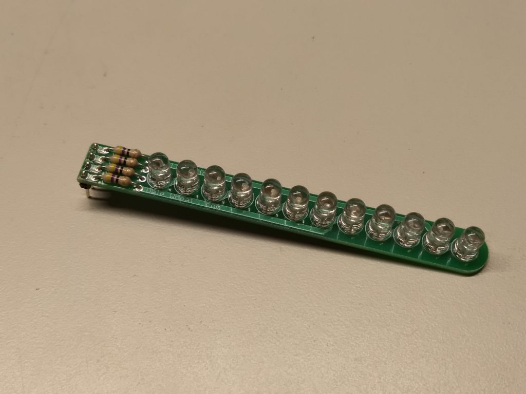
The 12LEDstick is a multiplexed (specifically Charlie-plexed) linear array of twelve bright blue LEDs. It uses four (4) pins to control all twelve LEDs, making it easy to add a lot of LEDs without dedicating a lot of valuable I/O lines. An Arduino library with example sketches is provided to make it easy to add to your next blinky project.
Why do it?
Adding multiple LEDs to a project makes it more visually interesting, useful and engaging. Using a clever multiplexing technique called Charlie-plexing allows up to 12 LEDs to be controlled with only four (4) signals. The LEDs can be mounted directly to the provided PCB for a compact linear array or wired individually to reach wherever you need extra blinky-ness!
Value/Benefit
Wiring up a lot of LEDs can require a correspondingly large number of connections and extra components. The 12LEDstick reduces this to four connections and four current-limiting resistors (provided). The Arduino library and examples sketches will get your project blinking fast and easy.
Who benefits?
Electronic hobbyists can easily add large numbers of LEDs to their projects without needing extra chips, shift-registers, resistors and wiring. Arduino builders can easily add more blinky bling without using up all the precious I/O lines. Any microcontroller that can sink or source 10mA per I/O pin can drive the 12LEDstick.
The 12LEDstick is a multiplexed linear array of blue 5mm LEDs that can be controlled with only four signals. An Arduino library and samples sketches are provided.
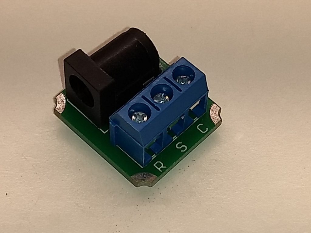
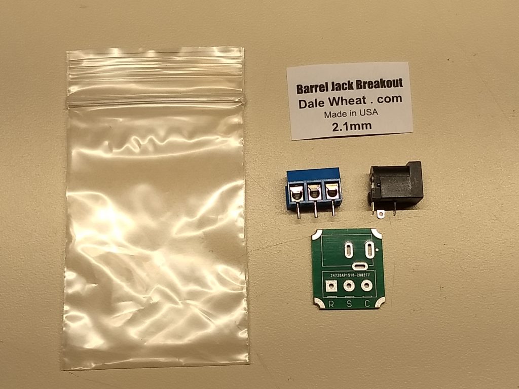
Today I have the pleasure to tell all you Good People that there is a new product available in the store. Without further ado, allow me to present the Barrel Jack Breakout board kit!
Barrel Jack Breakout
What is it?
Another “Hobbyist Tools†category product, the Barrel Connector Breakout PCB is small DIY kit that allows electronics hobbyists to use modular barrel connector in their project without having to solder to a female jack/receptacle. The connectors have center, outer and switch connections that are bought out to a 3 pin screw terminal. Mounting holes let you robustly and securely mount the power adapter to your project.
Why do it?
Having a solid, reliable power connection is critical for prototyping electronic projects. Using this adapter makes power connections easy and trouble-free. Have one less thing to worry about in your electronic experiments – keep several of these handy adapters on your bench!
Benefits & Values
Low-cost breakout board provides robust, convenient and reliable power connection for hobby electronics projects.
Who benefits from this kit?
Electronic hobbyists can easily and reliably power their projects. Prototyping engineers can quickly produce proof-of-concept designs. Classrooms can provide project power options that don’t require soldering.
Barrel Jack Breakout board kit (2.1mm variation shown)
What’s included in the kit?
Resealable plastic bag 2″x3″
Printed circuit board
Barrel jack connector (2.1mm or 2.5mm)
3-pin screw terminal block
Kit label
Barrel Jack Breakout Board Kit
The Barrel Jack Breakout kit provides a modular power connection for your project.
2.1mm and 2.5mm versions are available. Assembly is quick and easy. Once assembled, no soldering is required to install or use the Barrel Jack Breakout board with your breadboard project.
In the Before Times, if one of the products in the store was “Out of Stock”, it was not possible to place an order for it. Now some of the lower lead-time products can be backordered from the web store, even if today’s present inventory appears to be depleted.
Other products that have longer lead times, i.e., 30 days or more, are not available to be back ordered.
You Will Know Beforehand
If you place an order for a back ordered product, you will be notified before you place the order. Our intention and goal will be to ship any back ordered product within seven days. You will be notified if it looks like it will take longer than that. You will always have the option of cancelling any part of your order that has been back ordered.
Share Your Thoughts
As always, we really want to know what you think about this new policy change. The hope is that this will make it easier for you to get the products you want, when you want them.
In Part 1 of this series, I introduced you to the RISC-V computer instruction set architecture and described some first steps using an example device. In this article, I continue working with PlatformIO to program the GD32VF103CBT6 chip on the Sipeed Longan Nano development board. Specifically, we’ll use one of the onboard serial ports of the chip for both device programming and communication with the host PC.
Setup for Serial Communication
The GD32V series of chips from GigaDevice offer multiple bootloader options, including:
USB Device Firmware Update (DFU)
Serial bootloader using USART0 or USART1
The USB DFU method was demonstrated in the previous article. A “rolling†button press sequence on the Longan Nano board (“roll UP to UPloadâ€) puts the device in bootloader mode. This time, we’ll use a serial port to both program the device and communicate with the host PC.
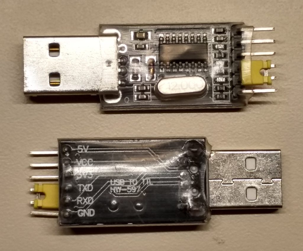
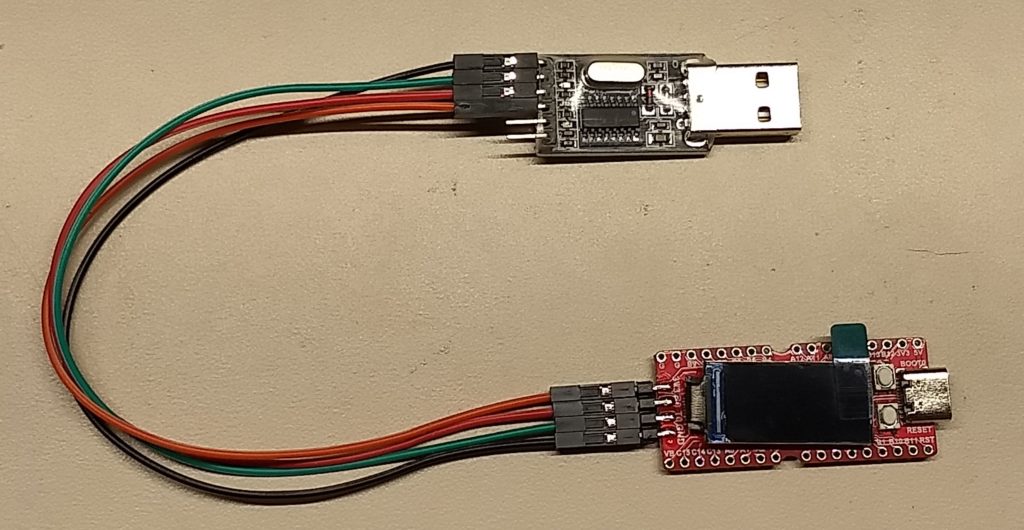
Two changes have to be made to switch over from USB to serial communication. First, we have to connect the serial port (USART0) on the GD32VF103 chip to the host PC via a USB-TTL adapter. You can use any adapter you like, as long as it provides an option to select the output voltage as being 3.3V, to be compatible with the GD32V chip. Here is a photo of the one I used:
USB-TTL adapter
Figure 1. The USB-TTL adapter will connect to the Sipeed Longan Nano. This model uses the CH430G interface chip.
Here are the necessary connections (color selection is entirely up to you):
USB-TTL —- Sipeed Longan Nano
3.3V, 3.3V, orange
GND, GND, black
TXD, R0, red
RXD, T0, green
Coonect the USB-TTL adapter to the Sipeed Longan Nano using four jumpers
Figure 2. Connect USB-TTL adapter to Sipeed Longan Nano. Note that transmit and receive are swapped on both ends.
Next, we change the upload_protocol specified in the project’s platformio.ini file from
upload_protocol = dfu
… to …
upload_protocol = serial
We need not indicate which port to use, baud rate or any other details like that. PlatformIO just figures it all out, which was nice.
I applied these changes first to the existing (and working!) example from the previous article that blinked all three colors of the on-board LED. It’s important to perform the “button roll†first, to prepare the chip for bootloading, before hitting the “Upload†icon. For short demonstration programs such as this, the time to program the device is still quite tolerable, even using the serial port.
A Bad Assumption
Here’s where a Bad Assumption came into play. Since the bootloader had to configure the on-board USART (universal synchronous/asynchronous receiver/transmitter) to communicate to the PC, I assumed that the USART would remain properly initialized, and that we could just start using it.
That turns out not to be the case. Which is OK, really. One shouldn’t depend on someone else’s software to set up one’s environment for one, should one? The bootloader looks to be doing a good job of covering its tracks as it hands off to the application program.
Create a New Project
Let’s create a new project for these further experiments with the Sipeed Longan Nano. In PlatformIO, go to the PlatformIO Home page. This page opens itself by default after you open the application, unless you tell it not to. If the Home page is not already being displayed, click on the PlatformIO icon (alien bug head?) on the left edge of the screen, then select “PIO Home/Open†from the Quick Access menu at the bottom left of the screen. There is also a Home icon on the bottom edge of the screen that looks like a little house. It can take a moment to load this page, because it has to contact the PlatformIO home planet.
On the left edge of the PlatformIO Home tab, you can select the Home icon, then find the “New Project†button in the Quick Access group at the top right. Alternatively, you can select the Projects icon and see a list of your current projects. The “Create New Project†button is at the top right of the screen.
Project Wizard
Either method brings up the Project Wizard dialog. Here you enter a project name and select which board to use. The list of supported boards is large and growing, so just start typing “longan nano†and it will start filtering out the non-matching options. This will pre-populate the “Framework†drop-down with “GigaDevice GD32V SDK†(what we want), as well as allow you to select “Arduinoâ€, which we will explore in a future article. Click the “Finish†button and your new project is set up for you.
Now you have an “empty†project for the GD32V framework, but it’s not really empty. There’s already a folder structure present that is well-organized for PlatformIO’s purposes. You can explore this structure using PlatformIO’s Explorer. Open the Explorer by clicking on the Explorer icon (stacked papers?) at the top left edge of the window.
Create a New Source File
In the Workspace section, expand the folder structure for your newly created project and find the “src†(source code) folder. Right-clicking on the “src†folder brings up a context menu. Select “New File†from this menu. You will see a blank line into which you should type the name of your source code. A good choice here would be “main.câ€, as it will contain our C program’s main() function, but feel free to express yourself. This will open a new editor with a tab at the top of the window.
Enter the following code into the editor
/* main.c
    part of GD32V-USART0 project
    Dale Wheat
    28 Feb 2020
*/

#include "gd32vf103.h"
#include <stdio.h>

int _put_char(int c) {
    usart_data_transmit(USART0, (uint8_t) c);
    while(usart_flag_get(USART0, USART_FLAG_TBE) == RESET);
    return c;
}

void main(void) {

    int i = 0; // iterator

    // initialize USART0

    rcu_periph_clock_enable(RCU_GPIOA);
    rcu_periph_clock_enable(RCU_USART0);
    gpio_init(GPIOA, GPIO_MODE_AF_PP, GPIO_OSPEED_50MHZ, GPIO_PIN_9);
    gpio_init(GPIOA, GPIO_MODE_IN_FLOATING, GPIO_OSPEED_50MHZ, GPIO_PIN_10);

    usart_deinit(USART0);
    usart_baudrate_set(USART0, 9600);
    usart_parity_config(USART0, USART_PM_NONE);
    usart_word_length_set(USART0, USART_WL_8BIT);
    usart_stop_bit_set(USART0, USART_STB_1BIT);
    usart_hardware_flow_rts_config(USART0, USART_RTS_DISABLE);
    usart_hardware_flow_cts_config(USART0, USART_CTS_DISABLE);
    usart_receive_config(USART0, USART_RECEIVE_ENABLE);
    usart_transmit_config(USART0, USART_TRANSMIT_ENABLE);
    usart_enable(USART0);

    while(1) {
        //usart_data_transmit(USART0, '!');
        printf("Hello, GD32V world!  i = %i\n", i);
        i++;
        for(volatile uint32_t n = 0; n < 10000000; n++); // delay
    }
}

// [end-of-file]
Listing 1. Test program for serial port testing
Once you’ve got this code into the editor, be sure to save it using either menu item “File/Save†or Ctrl+S.
Modify Project Configuration File
The Project Wizard created a basic project configuration file for you, named platformio.ini. Select this file using the Explorer and add the following two lines:
build_flags = -ffreestanding
upload_protocol = serial
Listing 2. Add these two lines to your project configuration file.
The first line, build_flags, allows you to send command-line options to the GCC compiler. You may have noticed that the main() function in this example is declared as returning “voidâ€, as is proper and fitting for an embedded application. The C programming language, originally developed for application programs, expects support from an operating system. The default and expected return value type is an “intâ€. To avoid the compiler complaining about this heretical behavior, we pass this option (-ffreestanding) to the compiler and all is well.
The second line, upload_protocol, is more important. Here we assign it a value of “serialâ€. PlatformIO does the rest.
Remember to save your newly-edited configuration file and then we’ll be ready to do a test build and make sure all the pieces are in place.
Time to Build
On the bottom edge of the screen is a toolbar we will find quite handy. To the right of the Home icon is the Build icon (check mark). Click this and PlatformIO will try to build your project. Ideally, you will see the following (or similar) text in the lower part of the window:
CONFIGURATION: https://docs.platformio.org/page/boards/gd32v/sipeed-longan-nano.html
PLATFORM: GigaDevice GD32V 1.1.2 > Sipeed Longan Nano
HARDWARE: GD32VF103CBT6 108MHz, 32KB RAM, 128KB Flash
DEBUG: Current (altera-usb-blaster) External (altera-usb-blaster, gd-link, jlink, rv-link, sipeed-rv-debugger, um232h)
PACKAGES:
 - framework-gd32vf103-sdk 1.0.0
 - toolchain-gd32v 9.2.0
LDF: Library Dependency Finder -> http://bit.ly/configure-pio-ldf
LDF Modes: Finder ~ chain, Compatibility ~ soft
Found 0 compatible libraries
Scanning dependencies...
No dependencies
Building in release mode
`buildhex' is up to date.
Checking size .pio\build\sipeed-longan-nano\firmware.elf
Advanced Memory Usage is available via "PlatformIO Home > Project Inspect"
RAM:   [=         ]   7.0% (used 2310 bytes from 32768 bytes)
Flash: [=         ]   6.5% (used 8456 bytes from 131072 bytes)
========================= [SUCCESS] Took 0.83 seconds ===============================================
Terminal will be reused by tasks, press any key to close it.
Upload the Newly Built Code
If all went well, we are ready to upload this test code to the device. Perform the bootloader “button roll†to prepare the device, then select the Upload icon (left arrow) in the toolbar. You should see this (very long) bunch of stuff appear in the Terminal window at the bottom of the screen:
Configuring upload protocol...
AVAILABLE: altera-usb-blaster, gd-link, jlink, rv-link, serial, sipeed-rv-debugger, um232h
CURRENT: upload_protocol = serial
Looking for upload port...
Auto-detected: COM15
Uploading .pio\build\sipeed-longan-nano\firmware.bin
stm32flash 0.4

http://stm32flash.googlecode.com/
Using Parser : Raw BINARY
Interface serial_w32: 115200 8E1
Version      : 0x30
Option 1     : 0x00
Option 2     : 0x00
Device ID    : 0x0410 (Medium-density)
- RAM        : 20KiB  (512b reserved by bootloader)
- Flash      : 128KiB (sector size: 4x1024)
- Option RAM : 16b
- System RAM : 2KiB
Write to memory
Erasing memory
Wrote address 0x08000100 (3.02%)
Wrote address 0x08000200 (6.05%)
Wrote address 0x08000300 (9.07%)
Wrote address 0x08000400 (12.09%)
Wrote address 0x08000500 (15.12%)
Wrote address 0x08000600 (18.14%)
Wrote address 0x08000700 (21.16%)
Wrote address 0x08000800 (24.19%)
Wrote address 0x08000900 (27.21%)
Wrote address 0x08000a00 (30.23%)
Wrote address 0x08000b00 (33.25%)
Wrote address 0x08000c00 (36.28%)
Wrote address 0x08000d00 (39.30%)
Wrote address 0x08000e00 (42.32%)
Wrote address 0x08000f00 (45.35%)
Wrote address 0x08001000 (48.37%)
Wrote address 0x08001100 (51.39%)
Wrote address 0x08001200 (54.42%)
Wrote address 0x08001300 (57.44%)
Wrote address 0x08001400 (60.46%)
Wrote address 0x08001500 (63.49%)
Wrote address 0x08001600 (66.51%)
Wrote address 0x08001700 (69.53%)
Wrote address 0x08001800 (72.56%)
Wrote address 0x08001900 (75.58%)
Wrote address 0x08001a00 (78.60%)
Wrote address 0x08001b00 (81.62%)
Wrote address 0x08001c00 (84.65%)
Wrote address 0x08001d00 (87.67%)
Wrote address 0x08001e00 (90.69%)
Wrote address 0x08001f00 (93.72%)
Wrote address 0x08002000 (96.74%)
Wrote address 0x08002100 (99.76%)
Wrote address 0x08002114 (100.00%) Done.
GET returns unknown commands (0x 6)
Starting execution at address 0x08000000... done.
================================= [SUCCESS] Took 2.22 seconds ===================================
Terminal will be reused by tasks, press any key to close it.
It’s interesting to me that PlatformIO uses the “stm32flash†program to upload the code. Here we see yet another similarity to the familiar STM32 family of parts from STmicroelectronics that we all know and love (or not). Unfortunately, the link given no longer computes. Also note that the reported RAM (20KiB) is incorrect, (-C8T6 instead of -CBT6?) but does not seem to affect the programming of the flash memory.
Testing the New Code
To see if the code is actually working or not, select the Serial Monitor toolbar icon (electrical plug? South-facing AND gate?). This will launch the serial communications program miniterm within the window at the bottom part of the screen. You should see “Hello, GD32V world!†followed by an ever-incrementing counter, about once a second:
Hello, GD32V world!  i = 300
Hello, GD32V world!  i = 301
Hello, GD32V world!  i = 302
Hello, GD32V world!  i = 303
Hello, GD32V world!  i = 304
Hello, GD32V world!  i = 305
Hello, GD32V world!  i = 306
Hello, GD32V world!  i = 307
Hello, GD32V world!  i = 308
Hello, GD32V world!  i = 309
Hello, GD32V world!  i = 310
Hello, GD32V world!  i = 311
Hello, GD32V world!  i = 312
Hello, GD32V world!  i = 313
Hello, GD32V world!  i = 314
Code Review
Let’s review the code a bit and see what we have.
After a short section of program comments identifying the file, project, author and date, we have a couple of #include statements:
#include "gd32vf103.h"
#include <stdio.h>
The first one defines all the interesting bits of the GD32VF103 chip, as far as pointers to peripherals and other useful information, as well as further linking to other files that bring in all the details about the standard peripheral library, which comes in handy presently.
The second statement gives us access to C’s standard IO (input and output) library, which includes the ever-popular printf() function.
Interfacing with printf()
To actually use the printf() function, we have to define a function called _put_char(). This is because the printf() function itself has no idea of where to send all those formatted characters. In this instance, we want to send them straight out the serial port known as USART0. This is the easiest port to use for this experiment, as these pins are brought out to the header on the edge of the Sipeed Longan Nano board.
The main() Function
From a programmer’s perspective, the fun starts with the main() function. In reality, some system initialization occurs before the main() function starts its work. This includes setting up the stack pointers, initializing the memory areas and cranking up the clock speed.
In our main() function, we declare an integer, i, that will be used as our loop counter later.
Next are the several steps necessary to properly initialize the serial port. This is accomplished using calls to the standard peripheral library, which takes a lot of tedium out of getting things working quickly.
Wake Up, Peripherals!
One thing that might be surprising to embedded programmers coming from, e.g., Arduino or Microchip PIC backgrounds is that almost all of the peripheral devices in the GD32V family, much like the embedded ARM devices, are powered off when the chip begins operation. Each peripheral must be explicitly enabled before use. This saves a lot of power, as unused sections of the chip remain dormant and take little or no power.
Additionally, since most pins of the GD32V device can be either inputs, outputs or serve as connections to the internal peripherals, you have to explicitly define which pins are used for what purposes. Only then do we get to the part where we can set up the individual peripherals to perform as we wish.
USART Configuration
There is a very particular sequence of events that must take place to properly get the USART up and running. All these steps are greatly simplified by using the standard peripheral library calls you see in the example program given. The parameters (9600 baud, 8 data bits, no parity, plus others) match the default communication settings of the miniterm program invoked by PlatformIO in its Serial Monitor function.
The Endless Loop
Most embedded applications follow a very simple pattern: perform some initialization, then go into a perpetual loop. This has been immortalized in Arduino’s setup() and loop() functions. We have our own infinite loop in our example, consisting of a while(1) control block. Since the constant “1†always evaluates to “true†by the C compiler, this loop will continue until something drastic happens. This could be an external reset, interrupt or ultimately power loss.
Within the loop, look for a statement that has been commented out, namely:
//usart_data_transmit(USART0, '!');
This was a call to the standard peripheral library that sent a single character to the USART for transmission. I used this for the first test of the program, before adding the printf() support. Upon opening the Serial Monitor, I was rewarded with a trail of exclamation points marching across the screen. Success!
Then Things Got Weird
Like Edison, I couldn’t be happy with my first glowing light bulb: I had to mess with it until it broke. Not surprisingly, this didn’t take long.
The first thing I tried was to increase the delay time between exclamation points. Simply adding a zero to the constant comparison value in the for() loop had no obvious effect on the pace of the points. Another zero also had no effect. More annoyed than puzzled, I proceeded with setting up support for formatted output using the printf() function from C’s standard input and output library.
Really Weird
Adding the printf() function support was simply a matter of adding the _put_char() function into the program. Nice! I was happy for many milliseconds as I watched my formatted “Hello, world!†statements scroll down the page. Oddly, however, the “i = 0†counter stayed at, oddly, zero. Did I forget to increment the variable? I’ve done that before. But no, that was not the case.
Some amount of time and head-scratching elapsed. This did not make sense. Surely I hadn’t run into some subtle compiler bug already. Then it hit me.
When Does i = 0?
The only time that the variable i should equal zero is right after the program starts… which happens to be right after the power comes on (or the reset button is pushed, which wasn’t happening). Glancing at the power LED on the Sipeed Longan Nano bard, I saw that it was flickering. Not good. And yet, it was good, as this would explain both the non-incrementing counter as well as the lack of timing changes induced by orders of magnitude different parameters previously seen.
Ultimately, the issue was that I had plugged the USB-TTL adapter into a USB hub, and not directly into my PC. It seems that the voltage drop through the hub, then through the voltage regulator on the USB-TTL adapter and then through the jumper wires to the development board resulted in a low-voltage condition for the system. Plugging the USB-TTL adapter directly into my PC solved the problem.
Conclusion
We now have two proven and (relatively) convenient methods to program the device: USB DFU and serial. Additionally, we have a bi-directional communication channel to the host PC that we can use for whatever we want, including simple debugging.
Another important advantage, which we had in the previous article but didn’t really explore, was access to the complete standard peripheral library for this device. This will obviate many hours of tedious research into datasheets, which will please some and annoy others.
Next Time
Continuing in this series of articles, I hope to explore a more in-depth method of debugging these chips. Stay tuned!
Things I Learned
PlatformIO is a rich environment that can be overwhelming at times, especially for new users. Additionally, there are almost always more than one way to accomplish any specific tasks, which is both useful and confusing.
Google Docs has a short but non-trivial learning curve for me. There are very few options when it comes to text styles. One of the default paragraph styles (“Normal textâ€) needed some extra space after each paragraph. This was easy to set using menu item “Format/Line spacing/Add space after paragraphâ€. Then selecting menu item “Format/Paragraph styles/Options/Save as my default styles†should make this change persistent.